LGA 1150
LGA 1150(Socket H3)是Intel於2013年推出的桌上型CPU插座,供Haswell及Broadwell微架構的處理器使用。[1]
| Socket H3 (LGA 1150) | ||
 | ||
| 規格 | ||
|---|---|---|
| 種類 | LGA | |
| 晶片封裝 | 覆晶技術 land grid array | |
| 接觸點數 | 1150 | |
| 總線協定 | DMI 2.0 | |
| 總線時脈 | ||
| 電壓範圍 | ||
| 處理器支援 | Core i3/i5/i7 (第四、五代) Xeon E3 Pentium Celeron | |
本文為CPU插座的一部份 | ||
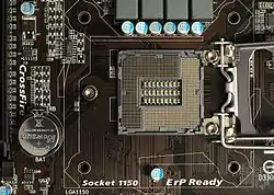
LGA 1150取代LGA 1155(Socket H2)。LGA 1150的插座上有1150個突出的金屬接觸位,處理器上則與之對應有1150個金屬觸點。散熱器的安裝位置則和LGA 1155和LGA 1156的一樣,安裝腳位的尺寸都是75mm × 75mm,因此適用於LGA 1156/LGA 1155的散熱器可以安裝在LGA 1150的插座上。[2]
和LGA 1156過渡至LGA 1155一樣,LGA 1150和LGA 1155的CPU互不相容。
晶片組
- Intel Z87/H87/H81/Q87/Q85/B85
- Intel Z97/H97
- Intel C222/C224/C226
| H81 | B85 | Q85 | Q87 | H87 | Z87 | |
| 超頻 | *CPU Ratio (ASRock, ECS, Biostar, Gigabyte, Asus, MSI[3][4][5][6][7][8]) + GPU | CPU + GPU + RAM | ||||
| Intel Clear Video Technology | 否 | 是 | ||||
| USB 2.0 / 3.0 | 10 / 2 | 12 / 4 | 14 / 6 | |||
| SATA 2 / 3 | 4 / 2 | 2 / 4 | 0 / 6 | |||
| CPU PCI-E | 1 × PCIe 2.0 ×16 | 1 × PCIe 3.0 ×16 | 1 × PCIe 3.0 ×16 或 2 × PCIe 3.0 ×8, 或 1 × PCIe 3.0 ×8 及 2 × PCIe 3.0 ×4 | |||
| 晶片組 PCI-E | 6 × PCIe 2.0 | 8 x PCIe 2.0 | ||||
| PCI | 否 | |||||
| Intel Rapid Storage Technology (RAID) | 否 | 是 | ||||
| Smart Response Technology | 否 | 是 | ||||
| Intel Anti-Theft Technology | 是 | |||||
| Intel Active Management, Trusted Execution, VT-d and vPro Technology | 否 | 是 | 否 | |||
| 發佈日期 | 2013年7月2日[9] | |||||
| TDP | 4.1W[10] | |||||
| 晶片製程 | 22nm | |||||
[11] Table updated with the latest information from Intel ARK
參考資料
- . [2012-07-04]. (原始内容存档于2012-08-26).
- . [2012-07-04]. (原始内容存档于2013-03-09).
- . [2013-08-30]. (原始内容存档于2014-01-09).
- . [2013-08-30]. (原始内容存档于2014-01-09).
- . [2013-08-30]. (原始内容存档于2014-01-09).
- . [2013-08-30]. (原始内容存档于2014-01-09).
- . [2013-08-30]. (原始内容存档于2014-01-09).
- . [2014-01-09]. (原始内容存档于2014-01-09).
- . [2013-08-30]. (原始内容存档于2014-01-09).
- (PDF). [2013-08-30]. (原始内容存档 (PDF)于2013-06-12).
- . [2013-08-30]. (原始内容存档于2016-03-04).
This article is issued from Wikipedia. The text is licensed under Creative Commons - Attribution - Sharealike. Additional terms may apply for the media files.
