NVIDIA Tesla
Tesla是一個NVIDIA的顯示核心系列品牌,主要用於伺服器高性能電腦運算,用於對抗AMD的FireStream系列。這是继GeForce和Quadro之后,第三个顯示核心商标。NVIDIA將顯示核心分為三大系列。GeForce用於提供家庭娛樂;Quadro用於專業繪圖設計;Tesla用於大規模的並聯電腦運算。
2007年開始使用的Tesla標誌 | |
| 研发者 | NVIDIA |
|---|---|
| 生产日期 | 2007年 |
| 类型 | 圖形處理器 |
Tesla以發明家尼古拉·特斯拉的名字命名。
產品系列
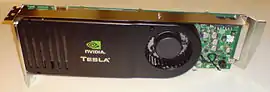
nVIDIA Tesla C870圖形處理器
目前,Tesla有三個系列:
- Tesla GPU运算处理器 - 外形與普通顯示卡大致相同,C870採用GeForce 8顯示核心,而C1060採用GeForce 200顯示核心,不設任何顯示輸出。
- Tesla GPU Deskside Supercomputer - 桌面平台用,外形與QuadroPlex相似,D870包含兩張C870运算处理器,可透過接線互联多個裝置。Tesla 10系列中沒有相關產品。
- Tesla GPU Server - 服务器用,外形與1U伺服器相似,S870包含四張C870运算处理器,而S1070包含四張C1060运算处理器,可透過接線互联多個裝置。
較早的時候,人們已意識到GPU能運算大量數據。所以开发者通过图形语言,利用顯示核心,來进行并行计算,亦即是GPGPU(通用繪圖核心)。但开发者需要有一定程度的图形处理知識,才能發揮顯示核心效能。隨後,NVIDIA推出了CUDA。开发者利用C++语言,再通過CUDA编译器,就能利用顯核運算。开发者可忽略图形处理技術,而直接利用熟悉的C++语言。开发者和科学家,就可以利用顯示核心,研究物理、生化和勘探等領域。
Tesla比較專注於高性能運算,并且C1060以上(G200)系列能支援双精度浮点格式。另一方面,CUDA被所有的NVIDIA顯示核心支援,包括GeForce和Quadro系列。
將來,顯示核心能普及化地,輔助中央處理器,進行视频压缩、数据库搜索等工作。並支援更多程式語言,例如Fortran、C++、JAVA和Python等
完整型號列表
| Model | 微架構 | Launch | Chips | Core clock (MHz) |
Shaders | Memory | Processing power (每秒浮點運算次數)[lower-alpha 1] | CUDA compute ability[lower-alpha 2] |
热设计功耗 (watts) |
Notes, form_factor | ||||||||
|---|---|---|---|---|---|---|---|---|---|---|---|---|---|---|---|---|---|---|
| Cuda cores (total) |
Base clock (赫兹) | Max boost clock (赫兹)[lower-alpha 3] |
Bus type | Bus width (位元) |
Size (吉字节) |
Clock (Transfer (computing)) |
Bandwidth (吉字节/s) |
單精度浮點數 (MAD+MUL) |
單精度浮點數 (MAD or 乘積累加運算) |
雙精度浮點數 (乘積累加運算) | ||||||||
| Units | MHz | MHz | W | |||||||||||||||
| C870 GPU Computing Module[lower-alpha 4] | Tesla (microarchitecture) | May 2, 2007 | 1× G80 | 600 | 128 | 1350 | 不適用 | GDDR3 | 384 | 1.5 | 1600 | 76.8 | 518.4 | 345.6 | 否 | 1.0 | 170.9 | Internal PCIe GPU (full-height, dual-slot) |
| D870 Deskside Computer[lower-alpha 4] | May 2, 2007 | 2× G80 | 600 | 256 | 1350 | 不適用 | GDDR3 | 2× 384 | 2× 1.5 | 1600 | 2× 76.8 | 1036.8 | 691.2 | 否 | 1.0 | 520 | Deskside or 3U 19-inch rack external GPUs | |
| S870 GPU Computing Server[lower-alpha 4] | May 2, 2007 | 4× G80 | 600 | 512 | 1350 | 不適用 | GDDR3 | 4× 384 | 4× 1.5 | 1600 | 4× 76.8 | 2073.6 | 1382.4 | 否 | 1.0 | 1U 19-inch rack external GPUs, connect via 2× PCIe (×16) | ||
| C1060 GPU Computing Module[lower-alpha 5] | April 9, 2009 | 1× GT200 | 602 | 240 | 1296[2] | 不適用 | GDDR3 | 512 | 4 | 1600 | 102.4 | 933.12 | 622.08 | 77.76 | 1.3 | 187.8 | Internal PCIe GPU (full-height, dual-slot) | |
| S1070 GPU Computing Server "400 configuration"[lower-alpha 5] | June 1, 2008 | 4× GT200 | 602 | 960 | 1296 | 不適用 | GDDR3 | 4× 512 | 4× 4 | 1538.4 | 4× 98.5 | 3732.5 | 2488.3 | 311.0 | 1.3 | 800 | 1U 19-inch rack external GPUs, connect via 2× PCIe (×8 or ×16) | |
| S1070 GPU Computing Server "500 configuration"[lower-alpha 5] | 1440 | 不適用 | 4147.2 | 2764.8 | 345.6 | |||||||||||||
| S1075 GPU Computing Server[lower-alpha 5][3] | June 1, 2008 | 4× GT200 | 602 | 960 | 1440 | 不適用 | GDDR3 | 4× 512 | 4× 4 | 1538.4 | 4× 98.5 | 4147.2 | 2764.8 | 345.6 | 1.3 | 1U 19-inch rack external GPUs, connect via 1× PCIe (×8 or ×16) | ||
| Quadro Plex 2200 D2 Visual Computing System[lower-alpha 6] | 2× GT200GL | 648 | 480 | 1296 | 不適用 | GDDR3 | 2× 512 | 2× 4 | 1600 | 2× 102.4 | 1866.2 | 1244.2 | 155.5 | 1.3 | Deskside or 3U 19-inch rack external GPUs with 4 dual-link DVI outputs | |||
| Quadro Plex 2200 S4 Visual Computing System[lower-alpha 6] | 4× GT200GL | 648 | 960 | 1296 | 不適用 | GDDR3 | 4× 512 | 4× 4 | 1600 | 4× 102.4 | 3732.5 | 2488.3 | 311.0 | 1.3 | 1200 | 1U 19-inch rack external GPUs, connect via 2× PCIe (×8 or ×16) | ||
| C2050 GPU Computing Module[4] | Fermi (microarchitecture) | July 25, 2011 | 1× GF100 | 575 | 448 | 1150 | 不適用 | GDDR5 | 384 | 3[lower-alpha 7] | 3000 | 144 | 否 | 1030.4 | 515.2 | 2.0 | 247 | Internal PCIe GPU (full-height, dual-slot) |
| M2050 GPU Computing Module[5] | July 25, 2011 | 不適用 | 3092 | 148.4 | 否 | 225 | ||||||||||||
| C2070 GPU Computing Module[4] | July 25, 2011 | 1× GF100 | 575 | 448 | 1150 | 不適用 | GDDR5 | 384 | 6[lower-alpha 7] | 3000 | 144 | 否 | 1030.4 | 515.2 | 2.0 | 247 | Internal PCIe GPU (full-height, dual-slot) | |
| C2075 GPU Computing Module[6] | July 25, 2011 | 不適用 | 3000 | 144 | 否 | 225 | ||||||||||||
| M2070/M2070Q GPU Computing Module[7] | July 25, 2011 | 不適用 | 3132 | 150.336 | 否 | 225 | ||||||||||||
| M2090 GPU Computing Module[8] | July 25, 2011 | 1× GF110 | 650 | 512 | 1300 | 不適用 | GDDR5 | 384 | 6[lower-alpha 7] | 3700 | 177.6 | 否 | 1331.2 | 665.6 | 2.0 | 225 | Internal PCIe GPU (full-height, dual-slot) | |
| S2050 GPU Computing Server | July 25, 2011 | 4× GF100 | 575 | 1792 | 1150 | 不適用 | GDDR5 | 4× 384 | 4× 3[lower-alpha 7] | 3 | 4× 148.4 | 否 | 4121.6 | 2060.8 | 2.0 | 900 | 1U 19-inch rack external GPUs, connect via 2× PCIe (×8 or ×16) | |
| S2070 GPU Computing Server | 不適用 | 4× 6[lower-alpha 7] | 否 | |||||||||||||||
| K10 GPU accelerator[9] | Kepler (微架构) | May 1, 2012 | 2× GK104 | 不適用 | 3072 | 745 | ? | GDDR5 | 2× 256 | 2× 4 | 5000 | 2× 160 | 否 | 4577 | 190.7 | 3.0 | 225 | Internal PCIe GPU (full-height, dual-slot) |
| K20 GPU accelerator[10][11] | November 12, 2012 | 1× GK110 | 不適用 | 2496 | 706 | 758 | GDDR5 | 320 | 5 | 5200 | 208 | 否 | 3524 | 1175 | 3.5 | 225 | Internal PCIe GPU (full-height, dual-slot) | |
| K20X GPU accelerator[12] | November 12, 2012 | 1× GK110 | 不適用 | 2688 | 732 | ? | GDDR5 | 384 | 6 | 5200 | 250 | 否 | 3935 | 1312 | 3.5 | 235 | Internal PCIe GPU (full-height, dual-slot) | |
| K40 GPU accelerator[13] | October 8, 2013 | 1× GK110B | 不適用 | 2880 | 745 | 875 | GDDR5 | 384 | 12[lower-alpha 7] | 6000 | 288 | 否 | 4291–5040 | 1430–1680 | 3.5 | 235 | Internal PCIe GPU (full-height, dual-slot) | |
| K80 GPU accelerator[14] | November 17, 2014 | 2× GK210 | 不適用 | 4992 | 560 | 875 | GDDR5 | 2× 384 | 2× 12 | 5000 | 2× 240 | 否 | 5591–8736 | 1864–2912 | 3.7 | 300 | Internal PCIe GPU (full-height, dual-slot) | |
| M4 GPU accelerator[15][16] | Maxwell (microarchitecture) | November 10, 2015 | 1× GM206 | 不適用 | 1024 | 872 | 1072 | GDDR5 | 128 | 4 | 5500 | 88 | 否 | 1786–2195 | 55.81–68.61 | 5.2 | 50–75 | Internal PCIe GPU (half-height, single-slot) |
| M6 GPU accelerator[17] | August 30, 2015 | 1× GM204-995-A1 | 不適用 | 1536 | 722 | 1051 | GDDR5 | 256 | 8 | 4600 | 147.2 | 否 | 2218–3229 | 69.3–100.9 | 5.2 | 75–100 | Internal MXM GPU | |
| M10 GPU accelerator[18] | 4× GM107 | 不適用 | 2560 | 1033 | ? | GDDR5 | 4× 128 | 4× 8 | 5188 | 4× 83 | 否 | 5289 | 165.3 | 5.2 | 225 | Internal PCIe GPU (full-height, dual-slot) | ||
| M40 GPU accelerator[16][19] | November 10, 2015 | 1× GM200 | 不適用 | 3072 | 948 | 1114 | GDDR5 | 384 | 12 | 6000 | 288 | 否 | 5825–6844 | 182.0–213.9 | 5.2 | 250 | Internal PCIe GPU (full-height, dual-slot) | |
| M60 GPU accelerator[20] | August 30, 2015 | 2× GM204-895-A1 | 不適用 | 4096 | 899 | 1178 | GDDR5 | 2× 256 | 2× 8 | 5000 | 2× 160 | 否 | 7365–9650 | 230.1–301.6 | 5.2 | 225–300 | Internal PCIe GPU (full-height, dual-slot) | |
| P4 GPU accelerator[21] | 帕斯卡 (微架构) | September 13, 2016 | 1× GP104 | 不適用 | 2560 | 810 | 1063 | GDDR5 | 256 | 8 | 6000 | 192.0 | 否 | 4147–5443 | 129.6–170.1 | 6.1 | 50-75 | PCI Express card |
| P6 GPU accelerator[22][23] | March 24, 2017 | 1× GP104-995-A1 | 不適用 | 2048 | 1012 | 1506 | GDDR5 | 256 | 16 | 3003 | 192.2 | 否 | 6169 | 192.8 | 6.1 | 90 | 行動PCI Express模組 card | |
| P40 GPU accelerator[21] | September 13, 2016 | 1× GP102 | 不適用 | 3840 | 1303 | 1531 | GDDR5 | 384 | 24 | 7200 | 345.6 | 否 | 10007–11758 | 312.7–367.4 | 6.1 | 250 | PCI Express card | |
| P100 GPU accelerator (mezzanine)[24][25] | April 5, 2016 | 1× GP100-890-A1 | 不適用 | 3584 | 1328 | 1480 | 高頻寬記憶體 | 4096 | 16 | 1430 | 732 | 否 | 9519–10609 | 4760–5304 | 6.0 | 300 | NVLink card | |
| P100 GPU accelerator (16 GB card)[26] | June 20, 2016 | 1× GP100 | 不適用 | 1126 | 1303 | 否 | 8071‒9340 | 4036‒4670 | 250 | PCI Express card | ||||||||
| P100 GPU accelerator (12 GB card)[26] | June 20, 2016 | 不適用 | 3072 | 12 | 549 | 否 | 8071‒9340 | 4036‒4670 | ||||||||||
| V100 GPU accelerator (mezzanine)[27][28][29] | 伏打微架構 | 1× GV100-895-A1 | 不適用 | 5120 | 未知 | 1455 | HBM2 | 4096 | 16 or 32 | 1750 | 900 | 否 | 14899 | 7450 | 7.0 | 300 | NVlink card | |
| V100 GPU accelerator (PCIe card)[27][28][29] | June 21, 2017 | 1× GV100 | 不適用 | 未知 | 1370 | 否 | 14028 | 7014 | 250 | PCIe card | ||||||||
| T4 GPU accelerator (PCIe card)[30][31] | 图灵微架构 | September 12, 2018 | 1× TU104-895-A1 | 不適用 | 2560 | 585 | 1590 | GDDR6 | 256 | 16 | 未知 | 320 | 否 | 8100 | 未知 | 7.5 | 70 | PCIe card |
| RTX A40[32] | 安培微架构 | 2020年10月5日 | ||||||||||||||||
| Model | 微架構 | Launch | Chips | Core clock (MHz) |
Shaders | Memory | Processing power (每秒浮點運算次數)[lower-alpha 1] | CUDA compute ability |
热设计功耗 (watts) |
Notes, form factor | ||||||||
| Cuda cores (total) |
Base clock (赫兹) | Max boost clock (赫兹)[lower-alpha 3] |
Bus type | Bus width (位元) |
Size (吉字节) |
Clock (Transfer (computing)) |
Bandwidth (total) (吉字节/s) |
單精度浮點數 (MAD+MUL) |
單精度浮點數 (MAD or 乘積累加運算) |
雙精度浮點數 (乘積累加運算) | ||||||||
Notes
- To calculate the processing power see Tesla (microarchitecture), Fermi (microarchitecture), Kepler (微架构), Maxwell (microarchitecture), or 帕斯卡 (微架构). A number range specifies the minimum and maximum processing power at, respectively, the base clock and maximum boost clock.
- Core architecture version according to the CUDA programming guide.
- GPU Boost is a default feature that increases the core clock rate while remaining under the card's predetermined power budget. Multiple boost clocks are available, but this table lists the highest clock supported by each card.[1]
- Specifications not specified by Nvidia assumed to be based on the NVIDIA GeForce 8GTX
- Specifications not specified by Nvidia assumed to be based on the NVIDIA GeForce 200
- Specifications not specified by Nvidia assumed to be based on the Quadro FX 5800
- With ECC on, a portion of the dedicated memory is used for ECC bits, so the available user memory is reduced by 12.5%. (e.g. 4 GB total memory yields 3.5 GB of user available memory.)
參考資料
- (PDF). January 2014 [7 December 2015]. (原始内容存档 (PDF)于2020-05-16).
- (PDF). Nvidia.com. [2015-12-11]. (原始内容存档 (PDF)于2020-11-24).
- . 31 October 2008 [January 29, 2017]. (原始内容存档于2012-02-26).
S1075 has one interface card
- (PDF). Nvidia.com. [2015-12-11]. (原始内容存档 (PDF)于2020-11-24).
- (PDF). Nvidia.com. [2015-12-11]. (原始内容存档 (PDF)于2020-11-24).
- (PDF). Nvidia.com. [2015-12-11]. (原始内容存档 (PDF)于2020-11-24).
- Hand, Randall. . VizWorld.com. 2010-08-23 [2015-12-11]. (原始内容存档于2020-08-17).
- (PDF). Nvidia.com. [2015-12-11]. (原始内容存档 (PDF)于2020-10-26).
- (PDF). Nvidia.com. [2015-12-11]. (原始内容存档 (PDF)于2020-11-24).
- (PDF). Nvidia.com. [2015-12-11]. (原始内容存档 (PDF)于2017-07-12).
- (PDF). Nvidia.com. [2015-12-11]. (原始内容存档 (PDF)于2020-03-26).
- (PDF). Nvidia.com. [2015-12-11]. (原始内容存档 (PDF)于2020-11-24).
- (PDF). Nvidia.com. [2015-12-11]. (原始内容存档 (PDF)于2020-06-17).
- (PDF). Images.nvidia.com. [2015-12-11]. (原始内容存档 (PDF)于2018-07-12).
- . Anandtech.com. [2015-12-11]. (原始内容存档于2020-11-08).
- . Devblogs.nvidia.com. 2015-11-10 [2015-12-11]. (原始内容存档于2017-07-09).
- (PDF). Images.nvidia.com. [2016-05-28]. (原始内容存档 (PDF)于2020-10-22).
- (PDF). Images.nvidia.com. [2016-10-29]. (原始内容存档 (PDF)于2017-05-10).
- (PDF). Images.nvidia.com. [2015-12-11]. (原始内容存档 (PDF)于2016-10-21).
- (PDF). Images.nvidia.com. [2016-05-27]. (原始内容存档 (PDF)于2020-10-22).
- Smith, Ryan. . Anandtech. 13 September 2016 [13 September 2016]. (原始内容存档于2021-01-16).
- (PDF). www.nvidia.com. [2019-03-07]. (原始内容存档 (PDF)于2020-07-28).
- . www.techpowerup.com. [2019-03-07]. (原始内容存档于2020-07-28).
- Smith, Ryan. . Anandtech.com. Anandtech.com. 5 April 2016 [5 April 2016]. (原始内容存档于2016-07-30).
- Harris, Mark. . [13 September 2016]. (原始内容存档于2017-05-07).
- Smith, Ryan. . Anandtech.com. 20 June 2016 [21 June 2016]. (原始内容存档于2020-11-11).
- Smith, Ryan. . Anandtech. 10 May 2017 [10 May 2017]. (原始内容存档于2020-11-12).
- Smith, Ryan. . Anandtech. 10 May 2017 [10 May 2017]. (原始内容存档于2020-11-12).
- Oh, Nate. . Anandtech.com. 20 June 2017 [20 June 2017]. (原始内容存档于2021-01-24).
- . NVIDIA. [17 October 2018]. (原始内容存档于2021-02-04).
- (PDF). www.nvidia.com. [2019-07-10]. (原始内容存档 (PDF)于2020-06-17).
- .
This article is issued from Wikipedia. The text is licensed under Creative Commons - Attribution - Sharealike. Additional terms may apply for the media files.
